The workspace window of the schematic editor contains components and transmission lines for use when adding schematic elements to a project. Once added to the current schematic, users can edit a transmission line's properties by either double-clicking on the desired element in the schematic window, or right-clicking on the desired element and selecting Edit Properties.
Each transmission line property editor includes element-specific settings, as well as the following general options:
- Name: user-defined component identifier.
- Label Position: placement of a component's label.
: determines which information is visible in a component's label.
- Enabled State: sets a component as either active or inactive. Inactive components are either open or short.
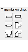
Ideal Transmission Lines
The
button adds a two-terminal ideal transmission line to the current schematic.
The
button adds a four-terminal ideal transmission line to the current schematic.
An ideal transmission line is defined by its admittance parameters as
\begin{equation}
Y_{11} = Y_{22} = \frac {1} {jZ_0 \tan (\beta l_p)}
\end{equation}
\begin{equation}
Y_{12} = Y_{21} = \frac {j} {Z_0 \sin (\beta l_p)}
\end{equation}
where $Z_0$ is the characteristic impedance, $\beta$ is the phase constant, and $l_p$ is the physical length of the line. The physical line length is calculated from the electrical length according to
\begin{equation}
l_p = \frac {l_e} {360} \lambda = \frac {l_e} {360} \frac {c} {2 \pi f}
\end{equation}
where $l_e$ is the electrical length in degrees, $c$ is the speed of light in a vacuum, and $f$ is the transmission line's evaluation frequency in Hz.
The following settings define the ideal transmission line parameters:
- Electrical Length: the electrical length, or phase length, defines the amount of phase shift an electromagnetic wave incurs while traveling over the length of the transmission line at a given frequency. The electrical length must be greater than zero.
- Characteristic Impedance: the characteristic impedance of the transmission line. The characteristic impedance must be greater than zero.
- Evaluation Frequency: the frequency at which the electrical length is defined. The evaluation frequency must be greater than zero.
Users should note that the two terminal ideal transmission line assumes that the reference terminal of both the input and output ports is connected to global ground resulting in the relationship shown in the image.
Substrate
Microstrip Line
The
button adds a microstrip line to the current schematic.
The microstrip’s quasi-static characteristic line impedance, $Z_0$, quasi-static effective dielectric permittivity, $\epsilon_{r,eff}$, and strip thickness effects are calculated using the formulas of [1].
The following settings define the microstrip line's parameters:
- Substrate: the microstrip’s substrate definition.
- Dispersion Model: the dispersion model the microstrip uses to calculate the frequency dependent characteristic line impedance and effective dielectric permittivity.
- Line Length: the physical length of the microstrip line defined in units of length. This quantity must be greater than zero.
- Line Width: the physical width of the microstrip line defined in units of length. This quantity must be greater than zero.
The $Z_0$ calculation of [1] is said to provide accuracy better than 0.01% for $\frac {W} {H} \leq 1$ and 0.03% for $\frac {W} {H} \leq 1000$.
The $\epsilon_{r,eff}$ calculation of [1] is said to provide accuracy better than 0.2% for $\epsilon_r \leq 128$ and $0.01 \leq \frac {W} {H} \leq 100$.
In accordance with reference information, the valid ranges for this component's parameters are described as $1 \leq \epsilon_r \leq 128$ and $0.01 \leq \frac {W} {H} \leq 100$, where $\epsilon_r$ is the substrate relative permittivity, $W$ is the microstrip line width, and $H$ is the substrate dielectric thickness.
Microstrip Step
The
button adds a microstrip step to the current schematic.
The capacitance and inductance of the microstrip step discontinuity are calculated using the formulas of [2]. The quasi-static characteristic line impedance, $Z_0$, quasi-static effective dielectric permittivity, $\epsilon_{r,eff}$, and strip thickness effects of line 1 and 2 are calculated using the formulas of [1].
The following settings define the microstrip step's parameters:
- Substrate: the microstrip step’s substrate definition.
- Dispersion Model: the dispersion model the microstrip uses to calculate the frequency dependent characteristic line impedance and effective dielectric permittivity of line 1 and line 2.
- $W_1$: the physical width of microstrip line 1 defined in units of length. This quantity must be greater than zero.
- $W_2$: the physical width of microstrip line 2 defined in units of length. This quantity must be greater than zero.
The schematic representation shows $W_1 \gt W_2$, but $W_2 \gt W_1$ is also acceptable. In such cases, the recommended range is $1.5 \leq \frac {W_2} {W_1} \leq 3.5$.
Users should note that the microstrip step is considered lossless.
In accordance with reference information, the valid ranges for this component's parameters are described as $1 \leq \epsilon_r \leq 10$ and $1.5 \leq \frac {W_1} {W_2} \leq 3.5$, where $\epsilon_r$ is the substrate relative permittivity.
Microstrip Tee
The
button adds a microstrip tee to the current schematic.
The microstrip tee utilizes an equivalent circuit model consisting of three microstrips, a shunt reactance, and two transformers as published by [3]. The quasi-static characteristic line impedance, $Z_0$, quasi-static effective dielectric permittivity, $\epsilon_{r,eff}$, and strip thickness effects of each microstrip line are calculated using the formulas of [1].
The following settings define the microstrip tee's parameters:
- Substrate: the microstrip tee’s substrate definition.
- Dispersion Model: the dispersion model the microstrip uses to calculate the frequency dependent characteristic line impedance and effective dielectric permittivity of line 1, line 2, and line 3.
- $W_1$: the physical width of microstrip line 1 defined in units of length. This quantity must be greater than zero.
- $W_2$: the physical width of microstrip line 2 defined in units of length. This quantity must be greater than zero.
- $W_3$: the physical width of microstrip line 3 defined in units of length. This quantity must be greater than zero.
The microstrip tee model is used for both symmetric and asymmetric junctions. Users should note that the microstrip tee considers dielectric and conductor loss as dictated by the calculated length of each of the three arms, as well as the substrate’s loss tangent, conductivity, and conductor thickness.
Reference [3] does not document any limitations on the microstrip tee, however, each of its three microstrip lines adheres to the same ranges described as valid for the microstrip line.
Microstrip Bend
The
button adds a 50% mitered microstrip bend to the current schematic.
The capacitance and inductance of the mitered bend discontinuity are calculated using the formulas of [4].
The following settings define the microstrip bend's parameters:
- Substrate: the microstrip bend’s substrate definition.
- Line Width: the physical width of the microstrip line defined in units of length. This quantity must be greater than zero.
Users should note that a 50% mitered bend is a reasonable approximation for all 90 degree bends, particularly mitered ones. The mitered bend shown in the image provides an explanation for different miter percentages.
Users should note that the microstrip bend is considered lossless.
In accordance with reference information, the valid ranges for this component's parameters are described as $2.36 \leq \epsilon_r \leq 10.4$ and $0.2 \leq \frac {W} {H} \leq 6$, where $\epsilon_r$ is the substrate relative permittivity, $W$ is the microstrip line width, and $H$ is the substrate dielectric thickness.
Microstrip Dispersion Models
The Kirschning/Jansen model calculates the frequency dependent characteristic line impedance, $Z_L(f)$, and frequency dependent effective permittivity, $\epsilon_r(f)$, using formulas from [5].
$\epsilon_r(f)$ is said to have an accuracy better than 0.6% for $0.1 \leq \frac {W} {H} \leq 100$, $1 \leq \epsilon_r \leq 20$, and $0 \leq \frac {H} {\lambda} \leq 0.13$ for frequencies up to 60 GHz and substrate thicknesses up to 25 mm.
$Z_L(f)$ is said to be valid for $0 \leq \frac {H} {\lambda} \leq 0.1$, $0.1 \leq \frac {W} {H} \leq 10$, and $1 \leq \epsilon_r \leq 18$.
In accordance with reference information, the valid ranges for this model are described as $1 \leq \epsilon_r \leq 20$, $0.1 \leq \frac {W} {H} \leq 100$, and $0 \leq \frac {H} {\lambda} \leq 0.13$, where $W$ is the microstrip line width, $H$ is the substrate dielectric thickness, and $\lambda = \frac {c} {f}$.
The Hammerstad/Jensen model calculates the frequency dependent characteristic line impedance, $Z_L(f)$, and frequency dependent effective permittivity, $\epsilon_r (f)$, using formulas from [1].
In accordance with reference information, the valid ranges for this model are described as $1 \leq \epsilon_r \leq 128$ and $0.01 \leq \frac {W} {H} \leq 100$, where $W$ is the microstrip line width and $H$ is the substrate dielectric thickness.
The Kobayashi model calculates the frequency dependent effective permittivity, $\epsilon_r (f)$, using formulas from [6].
This calculation of $\epsilon_r (f)$ is said to provide accuracy better than 0.6% for $0.1 \leq \frac {W} {H} \leq 10$ and $1 \leq \epsilon_r \leq 128$ with no frequency limits. Also, $Z_L (f) = Z_0$.
In accordance with reference information, the valid ranges for this model are described as $1 \leq \epsilon_r \leq 128$ and $0.1 \leq \frac {W} {H} \leq 10$, where $W$ is the microstrip line width and $H$ is the substrate dielectric thickness.
The Yamashita model calculates the frequency dependent effective permittivity, $\epsilon_r (f)$, using formulas from [7].
This calculation of $\epsilon_r (f)$ is said to provide accuracy better than 1% for $2 \leq \epsilon_r \leq 16$, $0.06 \leq \frac {W} {H} \leq 16$, and $0.1 \; GHz \lt f \lt 100 \; GHz$. Also, $Z_L (f) = Z_0$.
In accordance with reference information, the valid ranges for this model are described as $2 \leq \epsilon_r \leq 16$ and $0.06 \leq \frac {W} {H} \leq 16$, where $W$ is the microstrip line width and $H$ is the substrate dielectric thickness.
Microstrip Loss Calculations
Microstrip loss is calculated as a summation of dielectric and conductor losses according to
\begin{equation}
\alpha = \alpha_d + \alpha_c
\end{equation}
where $\alpha$ is the total attenuation constant, $\alpha_d$ is the attenuation due to dielectric losses, and $\alpha_c$ is the attenuation due to conductor losses.
Dielectric loss is calculated according to
\begin{equation}
\alpha_d (f) = \frac {\epsilon_r} {\sqrt {\epsilon_r (f)}} \frac {\epsilon_r (f)-1} {\epsilon_r -1} \frac {\pi} {\lambda} \tan (\delta_d)
\end{equation}
where,
$\epsilon_r =$ the relative permittivity of the substrate’s dielectric material
$\epsilon_r (f) =$ the frequency dependent effective permittivity of the microstrip
$\lambda = \frac {c} {f}$ is the wavelength
$\delta_d =$ the loss tangent of the substrate’s dielectric material
Users should note that if $\delta_d = 0$, then $\alpha_d(f) = 0$.
Conductor loss is calculated according to [2]. Loss due to surface roughness is incorporated into the calculation by applying a correction factor to the conductor’s skin resistance, $R_s$, such that [1][2]:
\begin{equation}
R_s (\Delta) = R_s \left\{ 1 + \frac {2} {\pi} \tan^{-1} \left[ 1.4(\frac {\Delta} {\delta})^2 \right] \right\}
\end{equation}
where $\Delta$ is the rms surface roughness and $\delta$ is the conductor’s skin depth.
Users should note that if the substrate’s conductivity equals 0 or the substrate’s conductor thickness equals 0, then $\alpha_c = 0$.
References
- E. Hammerstad and O. Jensen, “Accurate Models for Microstrip Computer-Aided Design,” Symposium on Microwave Theory and Technique, pp. 407-409, June 1980.
- R. Garg, I. Bahl, and M. Bozzi, Microstrip Lines and Slotlines, 3rd ed. Boston, MA, USA: Artech House, 2013, pp. 165 - 169.
- E. Hammerstad, "Computer-Aided Design of Microstrip Couplers with Accurate Discontinuity Models," Symposium on Microwave Theory and Techniques, pp. 54–56, June 1981.
- M. Kirschning, R. H. Jansen, and N. H. L. Koster, “Measurement and Computer-Aided Modeling of Microstrip Discontinuities by an Improved Resonator Method,” IEEE MTT-S International Microwave Symposium Digest, pp. 495–497, May 1983.
- M. Kirschning and R. H. Jansen, “Accurate Model for Effective Dielectric Constant of Microstrip with Validity up to Millimeter-Wave Frequencies,” Electronics Letters, vol. 8, no. 6, pp. 272–273, Mar. 1982.
- M. Kobayashi, “A Dispersion Formula Satisfying Recent Requirements in Microstrip CAD,” IEEE Transactions on Microwave Theory and Techniques, vol. 36, no. 8, pp. 1246–1250, Aug. 1988.
- E. Yamashita, K. Atsuki, and T. Ueda, “An Approximate Dispersion Formula of Microstrip Lines for Computer Aided Design of Microwave Integrated Circuits,” IEEE Transactions on Microwave Theory and Techniques, vol. 27, pp. 1036–1038, Dec. 1979.