XF reads both ODB++ database and .brd files, allowing users to import printed circuit board (PCB) geometry from circuit layout design tools, such as Cadence's Allegro PCB Design package. XF enables the customized construction of three-dimensional PCB representations and facilitates the data exchange between many applications in the PCB industry.
Check XF Application Preferences
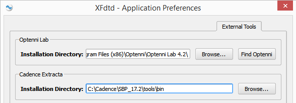
The location of Cadence's extracta executable is required in order to open Allegro .brd files so users must install Cadence's Allegro PCB Designer package on the machine running XF prior to setting the application preferences. XF cannot find and configure the executable automatically, so the location must be set manually by selecting Edit ❯ Application Preferences and working under the External Tools tab to specify the executable's directory under Cadence Extracta.
Importing an ODB++ database does not require any changes to XF's application preferences.
File Selection
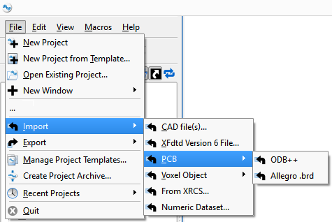
Users can import a PCB by selecting File ❯ Import ❯ PCB ❯ and choosing either ODB++ or Allegro .brd. A file selection window will appear, where users can navigate to the ODB++ directory or Allegro .brd file to import, as well as control some aspects of import behavior via the Advanced Options dropdown menu, if desired. Once the file or directory is chosen, the PCB data is read from disk and a preview is prepared and shown in the PCB import window.
PCB Import Window
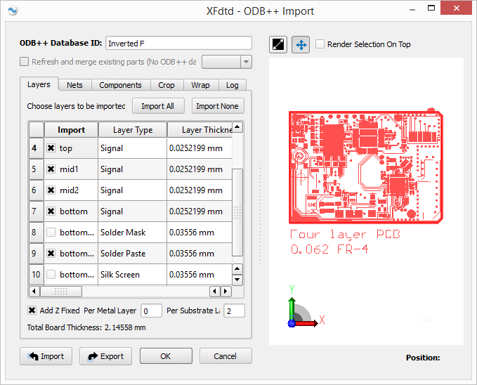
Once the preview is loaded, the PCB import window will open, where tabs and columns provide the available import options. One or more selections made on the left side of the window are displayed on the right side of the window for visualization purposes. The Board ID enables XF to identify solid geometry as either an ODB++ database or .brd file to use for the merging function, and it appears as the assembly name in the project tree.
The Refresh and merge existing parts option should be checked when users wish to update an existing PCB assembly with a new version of the file. With the option selected, XF imports the new file and combines it with the existing PCB assembly while maintaining material assignments, grid definitions, and other modifications set by the user. This option is grayed out if no existing database files are found in the XF project.
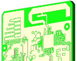
The preview pane on the right side of the window displays a flat preview of the PCB geometry. Visibility by layer and geometry type are determined by the controls in the preview tab. Selections in the nets and components tabs appear highlighted in the preview pane, regardless of the current preview tab visibility controls. The Zoom to Extents tool adjusts the view to include the space to which the import extends.
The Pan and Zoom tool allows users to move the view closer or farther using the mouse wheel, or click and drag to move the import in any direction without rotating.
At the bottom of the window, the Import button imports settings that were previously exported and saved as an .xml file.
The Export button writes the tab settings to an .xml file. Users can import this file at a later time and avoid having to reselect the subsets.
Users should note that the import and export settings .xml file format is not backward compatible with XF versions released prior to 7.11.1.
Layers Tab
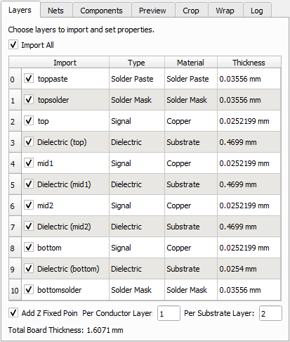
The Layers tab lists the PCB layers contained in the imported file and their properties in descending order, starting from the top layer. Users can select the layers to import and modify their thickness.
The Import column displays the name of each layer and a checkbox. Users decide which layers to import into XF by checking the box associated with each desired layer. The Import All checkbox can be used to toggle import on or off for all layers.
The Type column categorizes the layers according to specifications associated with the imported file type. Both .brd files and ODB++ databases require that each layer be assigned a type. There are eight possible layer designations in XF:
| Layer Type | Description |
|---|---|
| Signal | Indicates a conducting layer on which signals are routed. |
| Plane | Indicates a conducting ground plane layer. |
| Dielectric | Indicates substrate layers. |
| Solder Mask | Indicates a dielectric mask layer for applying solder paste. |
| Solder Paste | Indicates a layer for solder paste applied on top of pads, to which components are mounted. |
| Silk Screen | Indicates the ink layer occasionally applied on the top and/or bottom of the PCB. |
| Document | Indicates layers not included in the physical board, such as engineering drawings or text. |
| Unknown | Indicates a layer for which a type was undetermined. |
The Material column displays the material associated with each layer. For .brd files, materials are generated and assigned to each layer based on material property information in the file, if present. For ODB++, default materials are and assigned to each layer, since the ODB++ format has no material property information attached to layers. The materials will be added to the project and assigned to the relevant parts. The material properties can be edited through XF's material editor after they are added to the project.
The Thickness column displays the thickness of each layer. Users can edit the thickness values, if desired.
Below the tab's columns, the Add Z Fixed Points option determines whether or not manual fixed points are added to the grid per layer in order to resolve the geometry adequately in the mesh. By default, the checked option activates the Per Conductor Layer and Per Substrate Layer fields so that users can enter the desired value for each. Both fields are inactive when the option is unchecked.
The Total Board Thickness displays the sum of the imported file's conductor and substrate layers.
Nets Tab
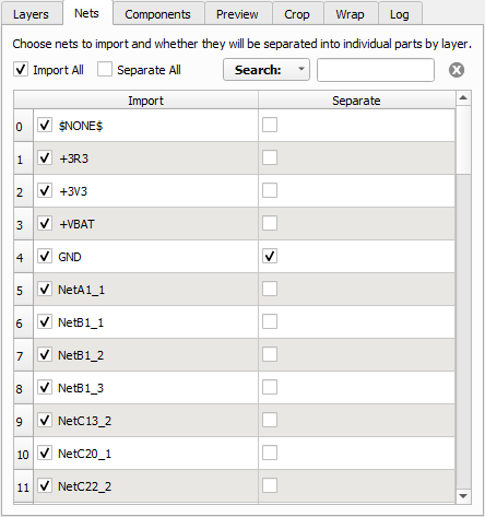
The Nets tab lists the PCB nets contained in the imported file. Users decide which nets to import into XF by checking the box associated with each desired net. Users must import the desired nets, as well as all layers on which they appear, in order to successfully import the entire net. The Import All checkbox can be used to toggle import on or off for all nets.
Users can manually enter text into the Search field and use the drop-down arrow to access additional filtering criteria.
The Search Type determines what search terminology is considered valid:
- Simple: default search for case insensitive text matches, which are displayed as terms are entered.
- Regular Expression: case insensitive search for multiple terms separated by a vertical bar without spaces, and followed by pressing Enter.
When choosing the Regular Expression search, users should note that entering a space either before or after a vertical bar returns incomplete search results. The Search These Fields options specify which fields are searched for the terms entered in the Search bar. The import comumn is the only available selection, and it includes fields with either numeral or text entries.
Imported PCBs will create a single conductor part across all layers for each net by default, so the import window includes a Separate column. Users can check the box associated with each net for which they would like to import separate parts for each layer. The Separate All checkbox can be used to toggle separation on or off for all nets.
Components Tab
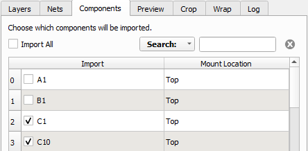
The Components tab lists the PCB circuit components contained in the imported file. Only the two-pin components that are identifiable as simple resistors, inductors, capacitors, switches, and diodes are selected for import by default, but users can change these selections by either checking or unchecking the circuit components as desired. The Import All checkbox can be used to toggle import on or off for all components. Components that do not have two pins will fail to be imported, if requested.
Users can manually enter text into the Search field and use the drop-down arrow to access additional filtering criteria.
The Search Type determines what search terminology is considered valid:
- Simple: default search for case insensitive text matches, which are displayed as terms are entered.
- Regular Expression: case insensitive search for multiple terms separated by a vertical bar without spaces, and followed by pressing Enter.
When choosing the Regular Expression search, users should note that entering a space either before or after a vertical bar returns incomplete search results. The Search These Fields options specify which fields are searched for the terms entered in the Search bar. The import comumn is the only available selection, and it includes fields with either numeral or text entries.
Users should note that each listed circuit component also has an associated circuit component definition. For resistors, inductors, and capacitors, a definition with the associated value will be created if possible. Otherwise, default component definitions will be used. Users can edit the circuit component definitions once they are added to the project.
Preview Tab
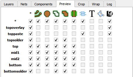
The Preview tab contains controls for the visibility of layers and types of geometry in the preview pane. Users can toggle visibility for each layer and type using the checkboxes to display only the geometry relevant to them. If a checkbox is disabled, it indicates there is no geometry of that type on that layer. The available geometry visibility types are, from left to right:
- Trace: conductor geometry for routing signals
- Pad: conductor geometry at trace endpoints and component mount locations
- Surface (outline): geometry for ground planes, solder mask, or other shapes (displays outline only)
- Surface (filled): geometry for ground planes, solder mask, or other shapes (displays solid shape)
- Via: indicates locations for drills that connect nets between layers
- Component: lines indicating the locations of two-pin components
- Text: geometry that was classified as text
- Wire: 2D wireframe geometry
- Misc: other geometry such as solder paste or otherwise uncategorized geometry
Crop Tab
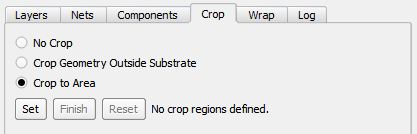
The Crop tab provides three options for importing subregions rather than the entire board:
- No Crop: default option that imports the entire board.
- Crop to Profile: removes any geometry that exists outside the profile bounds of the PCB.
- Crop to Area: allows users to specify one or more subregions to import.
Selecting Crop to Area enables the Set, Finish, and Reset buttons. The Set button provides two modes for defining polygon-shaped subregions, and applies the following options:
- Freehand line mode is the default behavior. Left-click the mouse to draw the polygon, right-click to close the current polygon and begin drawing another one, or use the following hotkey options:
- v: draws vertical lines (y-axis aligned).
- h: draws horizontal lines (x-axis aligned).
- o: draws lines orthogonal to the previous line once at least one line segment has been drawn.
- r: switches to rectangle mode, which is only available if a polygon has not been started.
- Ctrl+ click: deletes a polygon.
- Rectangle mode is the secondary method. Left-click once to start the rectangle and again to finish it, or use the following hotkey options:
- Ctrl+ click: deletes a polygon.
- f: returns to freehand mode.
Either clicking Finish or pressing Esc closes out the options for defining polygons, and clicking Reset deletes all polygons.
- Zoom the view during specification using the mouse wheel.
- Pan by holding the Shift key while clicking the mouse.
- Under the Nets tab, choose nets to be rendered before defining polygons for better visibility while drawing.
Wrap Tab
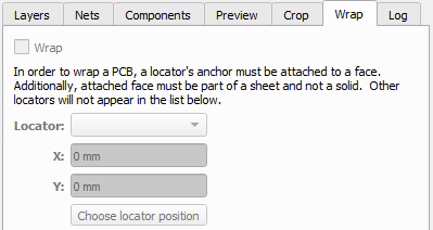
The Wrap tab includes options for creating flexible PCB geometry while importing either a .brd file or ODB++ database. Both formats provide a flat representation of the PCB that can be wrapped onto a target that must be created as a sheet, not a solid, before beginning the import process.
When checked, the Wrap option at the top of the tab enables the following settings:
- Locator: defines the target orientation through a drop-down menu of existing locators. A locator must be created before beginning the PCB import process, and have an anchor that is attached to a face.
- X and Y coordinates: defines the PCB source orientation using the entered values.
- Choose locator position: graphically defines the PCB source orientation.
Log Tab
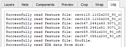
The Log tab displays output from either Cadence extracta or the ODB++ database. This is where any errors while creating a 2-D shape will be reported.
Advanced Options
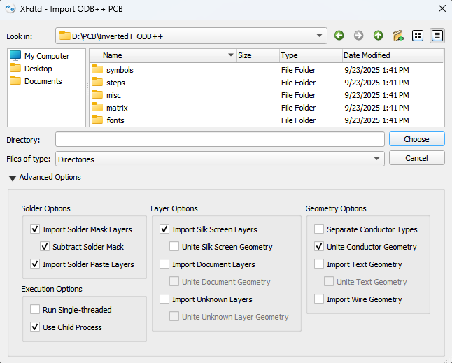
The Advanced Options give users control over which geometry and layers are imported and how they're processed. These must be configured before selecting the PCB file, and preferences will be saved for future imports. Some options are suboptions that activate only when their parent is enabled. Note that certain options can significantly slow imports on complex PCBs. Hover over any option in XF for detailed descriptions.
The Solder Options section determines how solder mask and paste layers are handled.
- Import Solder Mask Layers: by default, this enabled option classifies and imports solder mask layers.
- Subtract Solder Mask: by default, this enabled option subtracts solder mask shapes from the PCB profile shape in order to create a negative mask layer.
- Import Solder Paste Layers: by default, this enabled option classifies and imports solder paste layers.
The solder paste layers, if present, will be used to attach circuit components imported with the PCB.
If not present, components will be attached to the top and bottom conducting layers instead.
The Layer Options section determines which additional types of layers are imported, and whether geometry for those layers should be combined.
- Import Silk Screen Layers: by default, this enabled setting classifies and imports silk screen layers.
- Unite Silk Screen Geometry: when enabled, silk screen layer geometry is boolean united.
- Import Document Layers: when enabled, non-physical document layers are classified and imported.
- Unite Document Geometry: when enabled, document layer geometry is boolean united.
- Import Unknown Layers: when enabled, all encountered layers of unknown type are imported.
- Unite Unknown Layer Geometry: when enabled, unknown type layer geometry is boolean united.
The Geometry Options section offers some additional controls for how certain types of geometry are handled.
- Unite Conductor Geometry: by default, this enabled setting controls whether conductor parts are boolean united.
- Separate Conductor Types: when enabled, conductor geometry is imported in separate trace, pad, and surface parts, rather than a single part.
- Import Text Geometry: when enabled, text geometry (on any layer) is imported.
- Unite Text Geometry: when enabled, text geometry is boolean united.
- Import Wire Geometry: when enabled, 2D wireframe geometry (on any layer) is imported as Sketch parts.
The Execution Options section determines how XF handles the geometry processing. For best performance, these options should not be changed.
- Run Single-threaded: when enabled, PCB import operations run in single-threaded mode (by default, the process is multi-threaded).
- Use Child Process: by default, this enabled setting offloads some complex modeling operations to a child process in order to improve performance.