This example demonstrates XF's workflow for analyzing a matching network then applying it to full-wave FDTD results.
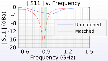
This workflow example includes an inverted-L antenna designed for a cellular application at LTE Band 5 operating from 824 MHz to 894 MHz. An FDTD simulation determines the intrinsic impedance of the antenna and then a wideband matching network is applied during post-processing in order to view the matched performance of S11, system efficiency ($e_s$), and far zone radiation.
The steps in the antenna design workflow form the basis for this project, however, this example focuses on the following aspects.
- The geometry includes the ground and the antenna.
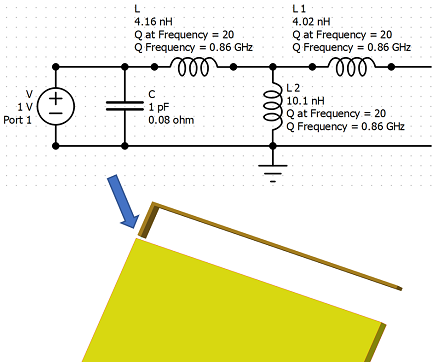
- An unmatched voltage source excites the antenna.
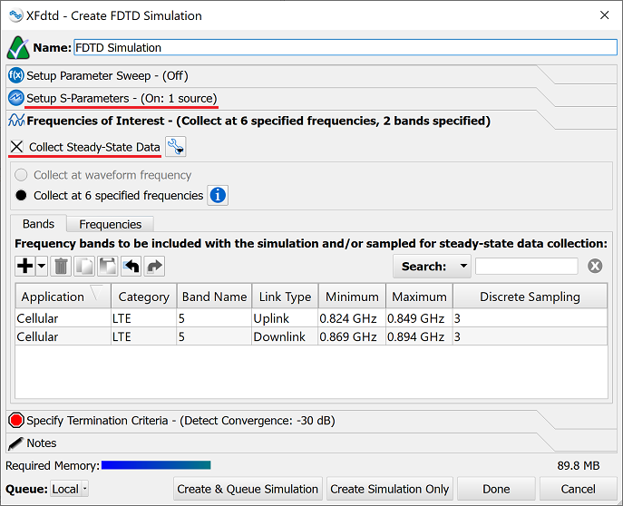
- An FDTD simulation requesting S-parameters with multiple steady-state frequencies is created.
- In post-processing, a schematic is created for computing the matched S11 and system efficiency results.
- The schematic is applied to the FDTD simulation to view the matched far zone radiation pattern.
Geometry
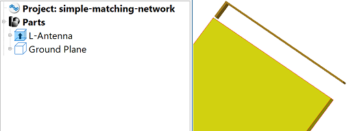
All required geometry must be added to the parts list in order to compute the intrinsic impedance of the antenna. This example consists of a ground plane created as a cuboid, and an inverted L-antenna created as an extrude. A gap separates the base of the antenna and ground plane.
This example's geometry is created and defined using the following specifications:
- The ground plane, or cuboid, has a width of 70 mm, depth of 150 mm, and height of 1 mm.
- The gap between the ground plane and inverted L-antenna is 0.5 mm.
- The inverted L-antenna is created as a 1 mm extrude.
- The antenna's base has a height of 5.5 mm and width of 1 mm.
- The antenna has a length of 70 mm and width of 0.5 mm.
Material
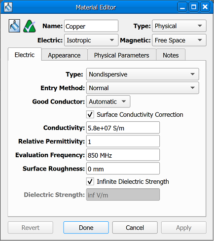
The ground plane and the antenna are each assigned a nondispersive material definition representing copper with a conductivity of 5.8e7 S/m and relative permittivity of 1. The material definition has surface conductivity correction enabled and the evaluation frequency set to 850 MHz.
Excitation
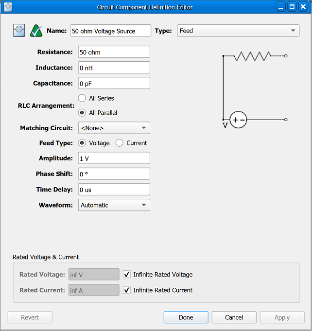
A circuit component is placed in the gap between the antenna and ground plane. Its associated definition specifies a voltage source with 50-ohm internal resistance and applies an XF-generated waveform to match the project's frequency of interest covering LTE Band 5.
Sensors
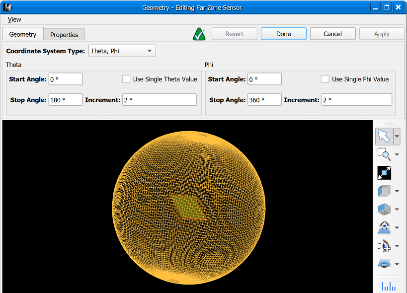
A far zone sensor saves the full, 3-D radiation pattern covering a theta range of 0 to 180 degrees in 2 degree increments, and a phi range of 0 to 360 degrees in 2 degree increments.
Although it requires no additional action, users should note that XF adds a port sensor requesting broadband S-parameters along with the circuit component, as well as a system sensor reporting system efficiency for each of the FDTD simulation's discrete frequencies.
Simulation
Prior to running an FDTD simulation, the remaining steps–material assignment, gridding, and meshing–in the antenna simulation workflow must be completed.
Running an FDTD simulation produces the antenna's unmatched full-wave results.
This example applies the following simulation settings:
- Compute S-parameters for a single, active feed.
- Collect steady-state data at six discrete frequencies across LTE Band 5.