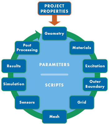
Every antenna simulation follows the same basic workflow, as shown in the image.
- Project properties: set the frequency range and display units.
- Geometry: import 3-D CAD files, import PCB databases, create geometry in XF, or modify existing geometry.
- Materials: specify electromagnetic properties of parts.
- Excitation: add voltage sources or modal field distributions.
- Outer boundary: apply perfectly absorbing boundaries on all sides, add a PEC ground plane, or use infinitely periodic boundaries.
- Grid: discretize the 3-D CAD space into cells.
- Mesh: associate a material with each cell edge and apply accuracy enhancements.
- Sensors: request results.
- Simulation: create and run a finite-difference time-domain (FDTD) simulation.
- Results: view output.
- Post-processing: analyze matching networks and apply weights with superposition for beamforming.
- Parameters: parameterize the project and perform parametric analysis.
- Scripts: customize the application by automating repetitive tasks or generating new output.
This discussion utilizes a microstrip patch antenna to illustrate the various steps.
Project Properties
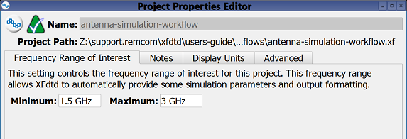
Project setup begins in the project properties editor, where the specified settings apply to the entire project and affect aspects such as geometry creation, cell size, waveforms, and output graphs. For antenna simulation, it is recommended that users set both the frequency range of interest and display units.
The frequency range of interest determines the minimum and maximum values that define the range over which users expect to retreive valid or relevant simulation results. This is typically specified as the range over which users want to analyze broadband S-parameter data, however, users can enter a single frequency if desired. Because XF utilizes the FDTD method, a single simulation produces broadband results over the entire frequency range. Specific discrete frequencies that require steady-state output are specified when creating the FDTD simulation in subsequent steps.
The settings under the display units tab define the default units shown throughout XF. This attribute offers convenient access to user preferences, such as inches versus centimeters. XF stores all data internally in backend units; these settings specify only how it appears in the user interface.
This patch example applies the following settings:
- Frequency range: 1.5 to 3 GHz
- Display units: frequency is set to GHz.
Geometry

Each project requires geometry that represents the device being simulated, but the level of detail depends on the antenna design stage. Early stages that identify major metals and investigate resonances require less detail than later stages that must include all relevant geometry for an antenna and its surroundings. For example, a solid PEC cuboid can sufficiently represent a ground plane during an early design iteration, but a fully-detailed multi-layer PCB becomes necessary as the stages advance.
This patch example's geometry is created using tools provided in XF:
- The microstrip and patch each utilize a sheet body.
- The substrate utilizes a cuboid.
- The ground plane utilizes a sheet body.
Materials
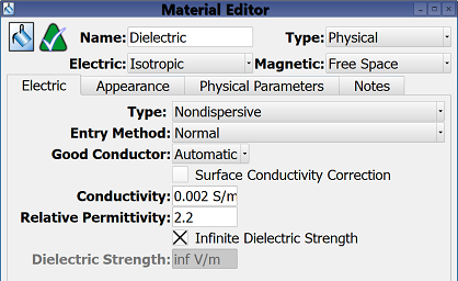
A material definition must be associated with each part in order to define its appearance and electromagnetic properties, so the necessary materials are first added to the project and then assigned to the desired part. The project tree's materials node allows users to define a set of electromagnetic properties once and use it in multiple places.
The most commonly used material for antenna design applications is an electric, isotropic, nondispersive type. In the material editor, relative permittivity and conductivity values are entered for dielectrics and metals. For metals, users should select the surface conductivity correction option and enter an evaluation frequency value, which is typically the center of the band.
There are two options for addressing wideband applications with material properties that are not constant for the frequency range. The first option is using a nondispersive type, however, the material properties change for low-, mid-, and high-band simulations. The second option is switching to a dispersive Debye-Drude definition with a complex permittivity that varies as a function of frequency. The dispersive material calculator assists with determining the material settings for a desired frequency response.
This patch example uses two nondispersive material definitions:
- Copper is assigned to the microstrip, patch, and ground plane.
- Conductivity of 5.98e+07 S/m.
- Surface conducivity correction is enabled with an evaluation frequency of 2 GHz.
- Dielectric is assigned to the substrate.
- Relative permittivity of 2.2.
- Conductivity of 0.002 S/m.
Excitation
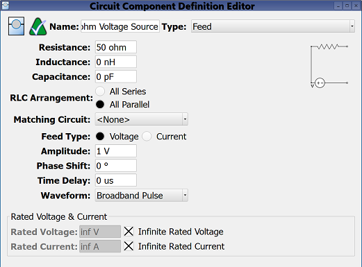
An excitation introduces energy into the simulation space and consists of three elements: location, electromagnetic properties, and waveform. There are two primary forms of input excitation—circuit components and waveguides—for antenna design applications, and the most appropriate choice depends on the desired field distribution at the source.
A circuit component excitation is a discrete source that is commonly used to connect a transmission line or antenna terminal to ground. Circuit components are either lumped with the excitation applied to a single FDTD cell edge, or distributed with the excitation spread across the area between the transmission line and ground. A distributed component is typically more accurate than its lumped counterpart.
A circuit component excitation consists of three distinct elements in the project tree:
- Circuit Component: defines the specific excitation location that is considered the port for which results are collected.
- Circuit Component Definition: specifies the electromagnetic properties—voltage or current source with internal resistance—associated with one or more circuit components.
- Waveform Definition: specifies the time-domain waveform and associated frequency-domain content applied to the circuit component.
The waveguide excitation—either modal or nodal—excites a transmission line's cross-sectional area with a field distribution, or mode. This provides support for additional transmission line types, such as a stripline, whose field distribution is not adequately modeled by a circuit component. A modal waveguide excitation applies a perfectly matched source at the excitation plane, and a nodal waveguide excitation introduces a mismatch during post-processing. The location and field distribution are specified in the modal and nodal waveguide editors, and a waveform is used in a manner similar to the circuit component excitation.
Waveguide excitations utilize a 2-D eigensolver to compute the field distribution, which is a process that depends on both the grid and mesh. If XF is unable to compute a mode, the gridding and meshing steps may need to be completed first.
This patch example's excitation consists of the following elements:
- Distributed circuit component located between the microstrip and ground.
- Feed circuit component definition specified as a voltage source with 50 Ω source resistance.
- XF-generated waveform definition spanning the project's frequency range of interest.
Outer Boundary
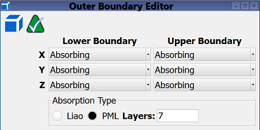
The outer boundary determines how the fields on the outermost cell edges of the finite simulation space are treated. Many antennas are simulated in free space, such as those against either a human head or phantom, but users can specify either an infininte PEC ground plane or infinitely periodic boundaries.
The following boundary conditions are relevant to antenna simulation:
- Six absorbing boundaries: simulates an antenna in free space. This common configuration is the default selection.
- Five absorbing boundaries with one PEC boundary: simulates an infinite PEC ground plane.
- Two absorbing boundaries with four periodic boundaries: simulates one unit cell of an infinitely periodic array.
This patch example's outer boundaries are set to absorbing on all six sides.
Grid
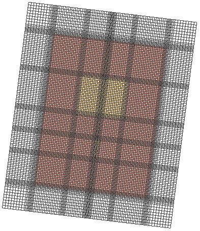
The grid discretizes the 3-D CAD space into Yee cells. Grid creation is a consequential step that impacts accuracy, run time, and RAM requirements, so XF utilizes the PrOGrid Project Optimized Gridding algorithm to achieve efficiency while allowing users to refine the grid in volumes of interest.
The grid depends on the project's frequency range of interest, geometric features, and material definitions. For antenna simulation, there are three primary aspects: small cell sizes that resolve volumes of interest, exact alignment between grid lines and the geometry of interest, and larger cell sizes elsewhere.
A simulation's accuracy is primarily driven by the use of small cell sizes for resolving important geometric features and capturing strong fields. Cells must be small enough to resolve design characteristics, such as a slot in an antenna or a small gap between conductors, in order to avoid an unintended electrical connection. The use of fixed points aligns the grid with geometry for proper resolution. Similarily, cells must be small enough to accurately capture high field variation around antennas and copper traces. Grid regions and boundary refinement assist with this as well.
Grid visualization tools assist in setting up and verifying an efficient grid.
This patch example's grid is defined by the following settings:
- Main grid editor settings:
- Minimum cells per wavelength: 35.
- Good conductor minimum feature size of 0.92 mm and 4 cells across to resolve the smallest microstrip width.
- Poor conductor minimum feature size of 1.2 mm and 5 cells across to resolve the subsrate thickness.
- Automatic fixed points are used for the microstrip, patch, and substrate.
Mesh
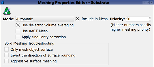
The mesh assigns a material to each cell edge in the grid. Built-in meshing order rules distinguish overlapping and coincident parts. Together, the grid and mesh comprise the geometric information passed to the calculation engine, so it's imperative that they accurately represent the 3-D CAD geometry.
Further, mesh properties for an individal part enable accuracy enhancements over traditional staircased meshes.
- Dielectric volume averaging (DVA) modifies the update equations at the interface between dielectric parts.
- Singularity correction captures highly varying field gradients at conductor edges.
- XACT Accurate Cell Technology® is a conformal, subcellular technique that splits the traditional Yee cell into multiple regions.
For antenna simulation, checking the mesh helps determine whether or not the correct electromagnetic properties are assigned to each part. Enabling DVA is recommended for dielectrics near the antenna, such as substrates and plastic housing. Enabling singularity correction and XACT is recommended for conductors connected to or near to the source, such as transmission lines and radiating elements.
This patch example's mesh is defined by the following settings:
- Singularity correction is enabled for the feed line, patch, and ground plane.
- Dielectric volume averaging is enabled for the substrate.
- XACT is not applied because the metal parts are planar, axis aligned, and snapped to the grid.
Sensors
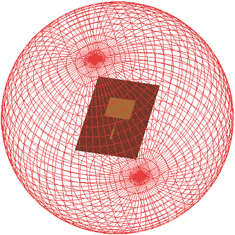
Sensors are objects that request results, and the sensor type determines which data is saved. Users should note that the list of frequencies for steady-state frequency requests is specified during simulation creation.
For antenna simulation, an array of sensors is specified according to the desired analysis:
- Port sensors are associated with circuit components or waveguides and return results that include input power and S-parameters.
- Near-field sensors collect data on points, planes, surfaces, or volumes in the simulation space.
- Far zone sensors utilize a near- to far-field transform to compute radiation patterns.
- Specific absorption rate (SAR) and SAR averaging sensors compute metrics for human exposure in compliance with IEC/IEEE international standards.
- System sensors are included in any simulation that collects steady-state data. It provides data that includes net available power, total dissipated power, and system efficiency.
This patch example included the following sensors:
- A port sensor associated with the voltage source collecting S-parameters.
- A planar sensor on the patch's surface collecting steady-state electric field data.
- A 3-D far zone sensor collecting a steady-state antenna radiation pattern.
- A system sensor collecting net input power and radiation efficiency.
Simulation
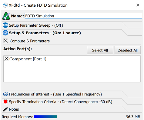
Once a completed project is saved, users can set up and run a calculation by creating an FDTD simulation. When creating a simulation, XF provides options for creating a parameter sweep, collecting S-parameters, and specifying the steady-state frequencies at which data is saved.
This patch example utilizes the following simulation settings:
- S-parameters are computed for a single port.
- Steady-state data is collected at 2.38 GHz.
Results
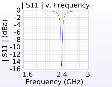
Once the simulation is complete, the data collected by the sensors during the calculation is available to view through the results browser. Results are primarily viewed on graphs, as field displays in the geometry view, or in tables.
This patch example includes the following generated output:
- S-parameters computed for 1.5 to 3 GHz.
- System efficiency and a 3-D radiation pattern at 2.38 GHz.
Post-Processing
XF's post-processing options enable further array and matching network analyses using the results of a completed FDTD simulation. The superposition simulation and array optimization options perform varius types of antenna array analysis by applying the electromagnetic principle of superposition. Together, they support numerous antenna designs, including phased arrays, multi-arrays, dual-polarized arrays, and subarrays. Scripts are also available for analyzing codebooks and computing incident power density.
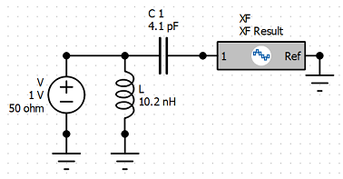
For matching network analysis, XF provides a schematic editor and frequency-domain circuit solver where an FDTD block is analyzed with RLC components. Once the topology and component values are determined, the circuit simulation feature combines a schematic and FDTD simulation in order to view all steady-state full-wave results with the schematic applied.
FDTD results are also exported from XF for post-processing in other programs, such as Matlab, ADS, or OptenniLab.
This patch example does not utilize any post-processing options.
Parameters

A parameter is a user-defined variable or equation that can be utilized in several steps throughout the workflow. Once a parameter is added in the parameters window, it can be entered into any editable field and applied to multiple objects—imported CAD parts, geometry modifications, material definitions, and grid. Any defined parameter listed in the parameters window is available for use when performing a parameter sweep when setting up a simulation.
For antenna simulation, parameters are commonly used to parameterize a variety of geometry dimensions and run parameter sweeps.
This patch example does not utilize parameters.
Scripting
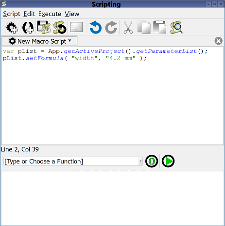
A script performs a specified task that could otherwise be done through the user-interface, and is often used to automate tedius or complicated tasks for improved efficiency. This customizable functionality can be utilized in several steps throughout the workflow and allows users to quickly perform repetitive tasks, reference external files, employ a series of modeling operations, or generate custom output.
This patch example does not utilize scripting.