XF's gridding algorithm allows users to apply PrOGrid Project Optimized Gridding®, enter the grid manually, or specify a combination of the two. Grid settings—along with the mesh settings—help discretize the CAD geometry into cell edges, creating a representation that is passed to the calculation engine for simulation. By following a standard workflow, users can reliably generate an efficient grid that balances the trade-off between accuracy and run time.
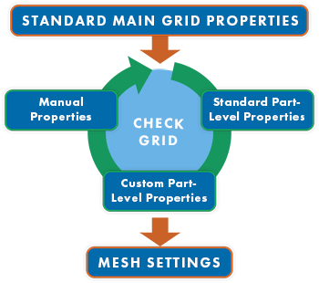
Upon completing the prerequisite steps in the project setup workflow, the gridding process begins in the main grid editor with settings that both define the main grid and provide default values for part-level gridding properties.
Next, an iterative process is utilized.
- Check grid: visualize the grid for alignment with geometry.
- Standard part-level properties: enable PrOGrid and automatic fixed points for the parts of interest.
- Advanced properties: apply custom PrOGrid settings at the part-level.
- Manual properties: selectively enter manual grid regions and fixed points in areas not properly resolved by PrOGrid.
Once the grid setup is complete, users can apply mesh settings to increase accuracy over traditional staircased finite-difference time-domain (FDTD) cells.
Prerequisite Steps
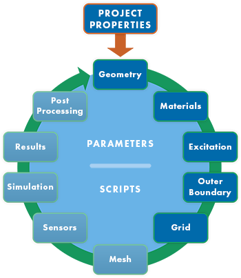
The simulation workflow includes a single gridding step with preceding steps that are required in order for XF's gridding algorithm to generate an optimal grid.
The frequency range of interest in the project properties editor impacts any value based on wavelength. For example, cells per wavelength in either free space or a dielectric, as well as the amount of free space padding, are evaluated within the defined range.
Geometry must be either created or imported into a project in order to consider certain characteristics that impact the grid, such as the location of good conductor edges that generate strong field gradients and the smallest geometry to resolve. Smaller cell sizes are necessary for resolving strong field values, and an adequate number of cells across gaps and traces is required for capturing the field variation in and around them. Additionally, identified geometry features, such as edge corners and bounding boxes, help ensure alignment with the gridlines.
Materials establish whether a part is a good conductor or poor conductor. This designation determines which settings and default values are applied to parts with PrOGrid enabled. Boundary refinement resolves high field variation on a good conducting part's edges, and padding extends base cells beyond a poor conducting part's bounding box. Additionally, permittivity values are used to determine the appropriate number of cells per wavelength inside dielectrics.
A circuit component or waveguide excitation impacts the grid when PrOGrid is applied. Enabling grid regions in either of these editors adds boundary refinements to reduce grid cell sizes near the excitation that are consistent with the grid editor's good conductor settings. For circuit components, grid regions ensure the distance between the two component endpoints by a minimum of one grid cell.
The outer boundary conditions determine how fields propagating toward the grid's outer edge are either absorbed or reflected, and affect the appropriate free space padding configuration when specifying the grid's extents. For example, zero padding might be preferable for a PEC ground plane in order to place a device directly on it.
Standard Main Grid Properties
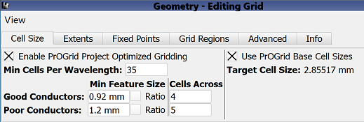
The gridding workflow begins in the main grid editor with entering values in the cell size tab. Users can also make specifications in the extents and advanced tabs as needed depending on the project.
Users should select the Enable PrOGrid Project Optimized Gridding and Use PrOGrid Base Cells Sizes options for most applications. Long-time XF users occassionally uncheck both of these options when they are comfortable with a different gridding workflow, however, the former setting is the only single access point for enabling or disabling PrOGrid project-wide.
Min Cells Per Wavelength controls the cell size both in free space and within dielectrics. Users should set this value based on knowledge from previous simulations. Ten cells per wavelength is the minimum allowable number due to FDTD stability criterion, and values up to 30 or 90 and above are common depending on the application.
The previous settings affect the largest allowable cell size in the absense of geometry, while the Min Feature Size and Cells Across settings impact the smallest cell size in the space. For PCB applications, the narrowest copper trace and thinnest dielectric layer are typically entered as minimum feature sizes. It is recommended that users uncheck each Ratio setting and manually enter the physical dimensions.
Users can move on to the check grid step for the majority of workflows, but in some cases might consider the extents and advanced tabs next.
The extents tab controls the amount of free space padding between the geometry's bounding box and the grid's outer boundary. The default values might require adjustments for lower frequency applications—NFC or MRI—or when either infinite PEC ground planes or periodic boundaries are used.
The advanced tab provides default values for part-level PrOGrid properties. Some applications—such as millimeter-wave antenna design—benefit from an increased boundary refinement ratio. This point in the gridding workflow is appropriate for applying advanced settings globally to all parts.
Check Grid
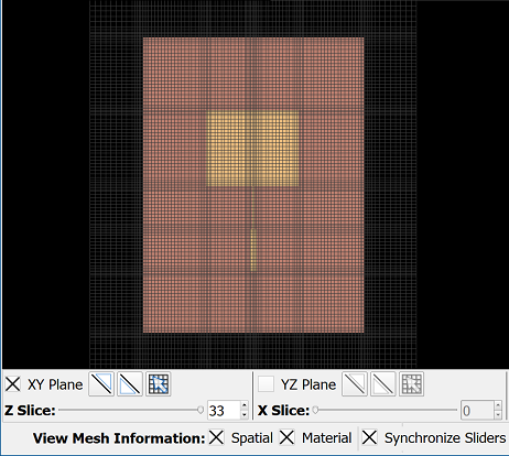
Visualizing the grid allows users to verify that the grid settings are applied as expected and the gridlines align with the geometry. Viewing the grid begins with the mesh controls that open across the bottom of the geometry window.
Once the grid is rendered and oriented along an axis, users can compare it to axis-aligned geometry and confirm that there is adequate resolution in the areas of interest. For example, users can count the visible number of cells across the parts used to set the Min Feature Size for both Good Conductors and Poor Conductors in order to verify that the Number of Cells Across value is correctly applied.
The grid visualization tools are used throughout the gridding workflow to ensure proper grid alignment with geometry.
Standard Part-Level Properties
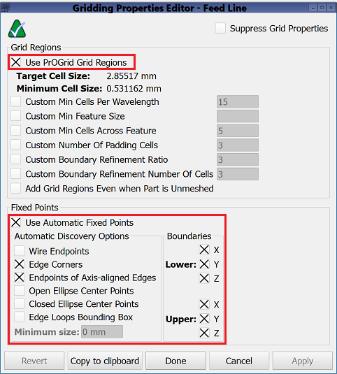
Setting part-level gridding properties begins with enabling the Use PrOGrid Grid Regions option for the parts of interest. This typically includes both good and poor conductors in the vicinity of strong electromagnetic fields, such as those parts near an antenna.
This setting is enabled by default for all parts as they are either imported or created. For projects containing hundreds or thousands of parts, this could generate a grid that is unnecessarily dense throughout the entire simulation space. In such cases, it is more efficient to disable PrOGrid for all parts in either the entire project or an assembly, and then enable it again for only the parts of interest.
Once PrOGrid is enabled for the appropriate parts, misalignment between gridlines and geometry must be addressed by selecting the Use Automatic Fixed Points option. When selected, the gridding algorithm attempts to align gridlines with geometric attributes, such as edge corners and bounding boxes.
Custom Part-Level Properties
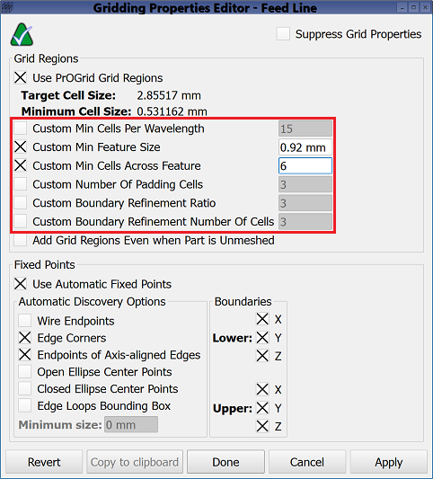
The previous steps generate a sufficiently accurate grid in the majority of XF's applications, but properly resolving geometric features could require additional settings. Users can resolve the grid in relation to an individual part by applying custom PrOGrid settings at the part level.
This is relevant in the following instances:
- Resolving a part's geometric feature using custom settings for feature size and cells across.
- Resolving the separation between two parts using custom settings for boundary refinement ratio.
- Resolving the volume around a part using cells per wavelength and cells padding.
For increased efficiency when all or the majority of parts with PrOGrid enabled require the same custom settings, users can adjust the appropriate value in the main grid editor because its settings provide the default values for all parts.
Custom PrOGrid settings are applied to a part through it's gridding editor. Checkboxes in the Grid Regions section enable custom value fields that override specifications in the main grid editor.
Manual Properties
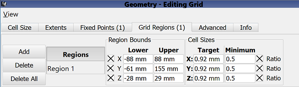
Similar to custom properties, manual properties allow users to fine-tune the grid for improved resolution and alignment. Manual properties operate outside of the PrOGrid algorithm and allow users to specify cell sizes within a volume and set the exact locations of gridlines. Manual properties are entered in both the main grid and part-level editors.
The main grid editor allows users to manually set fixed points and define grid regions. The manual Fixed Points specifications define the placement of a gridline and supersede the automatic part-level settings, allowing users to place gridlines in exact locations. The Grid Regions settings define a target cell size throughout a region, or volume.
The part-level grid editor specifies the target cell size associated with a part's bounding box. Unchecking Use PrOGrid Grid Regions and checking Enable Grid Regions provides settings that specify the target cell size and boundary extentions.
One example demonstrating the utility of these manual settings is 79 GHz radar applications requiring the thickness of a copper trace to be resolved. Specifying a minimum good conductor feature size of 15 um with one cell across in the main grid editor's cell sizes tab generates an unnecessarily small grid throughout the entire simulation space. Instead, users can populate the cell sizes tab with geometric information related to the width of the microstrip feed, and resolve the copper thickness locally with manual fixed points, grid regions, or part-level grid regions.
Mesh Settings
Mesh settings are a seperate step in the project setup workflow. Grid settings discretize the simulation space into cells, while the mesh specifies which material properties are associated with each cell edge and introduces accuracy enhancements over traditional FDTD update equations. Together, the grid and mesh comprise the geometric information passed to the calculation engine and create an accurate representation of the 3-D CAD geometry.
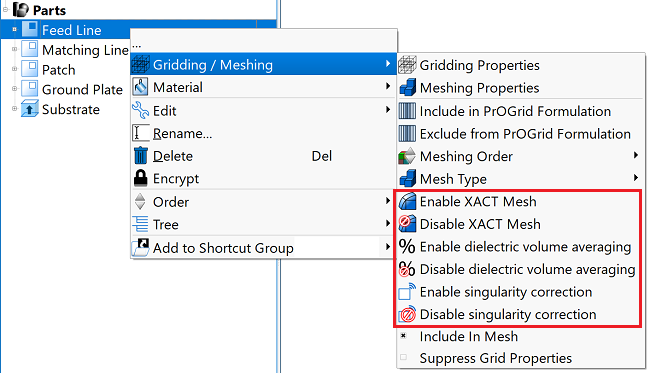
Users can enable accuracy enhancements using the following mesh settings:
- Dielectric volume averaging (DVA) modifies the update equations at the interface between dielectric parts.
- Singularity correction captures highly varying field gradients at conductor edges.
- XACT Accurate Cell Technology® is a conformal, subcellular technique that splits the traditional Yee cell into multiple regions.