Electrostatic discharge (ESD) analysis determines an electronic device's susceptibility to damage and failure from the current generated by an ESD event.
This analysis utilizes multiple aspects of an XFdtd project:
- Geometry: a device under test (DUT) is added to the project by importing a printed circuit board (PCB) or CAD model, or created using XF's modeling operations. A conducting ESD gun is also added and then grounded to a PEC outer boundary condition.
- Materials: dielectric strength must be defined for each material.
- Excitation: a user-defined waveform definition models the time-domain shape and strength of the discharged signal. The signal is injected into the simulation space through a current source.
- Circuit components: rated voltage and current values must be defined for each circuit component.
- Grid: gridding properties are set to resolve geometry features with sufficient accuracy.
- Sensors: dielectric breakdown sensors monitor cell edges for electric fields that exceed input parameters and identify locations where damage is likely.
- Simulation: S-parameters and steady-state data are disabled and settings are adjusted to ensure simulation time is sufficient to resolve the waveform.
- Results: areas of potential dielectric breakdown and circuit components susceptible to damage are reported and available for analysis through the results browser.
Geometry
A fully detailed DUT model is added to an XF project using the PCB and CAD import capability. In a lab, the DUT is often placed on a flat, grounded surface while the tests are performed. This setup is achieved in XF by using the PEC boundary condition and then manually adjusting the free space padding to zero cells in the desired direction.
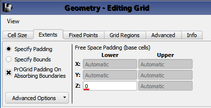
In the grid editor, entering zero cells as the free space padding positions the DUT such that it is lying on the PEC ground plane outer boundary.
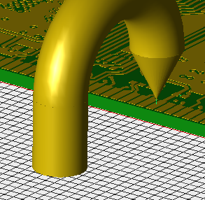
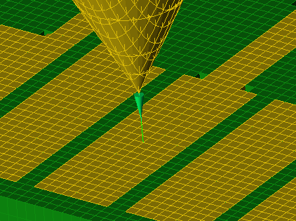
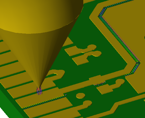
After the DUT geometry has been placed on the PEC ground plane, the ESD gun is constructed. In cases where the detailed ESD simulator geometry is of less importance than the DUT geometry, simplified ESD probe geometry can be used.
Care must be taken when placing the ESD probe to ensure that its base is on the same plane as the DUT's lower bounding box edge. This ensures that both the DUT and probe are appropriately attached to the PEC ground plane. If the probe's lower bounding box edge is higher than the DUT's, the probe will not be grounded. Conversely, if the probe's lower bounding box edge is lower than the DUT's, the DUT will not be grounded. After the ESD probe is placed, an ESD excitation can be created to connect the probe to the DUT at the test point.
Materials
Each material definition, such as an electric nondispersive material, includes a dielectric strength value that sets the maximum electric field it can withstand without experiencing dielectric breakdown, or losing its insulating properties. Checking every cell edge in the simulation space at each timestep negatively impacts simulation speed. As such, a dielectric breakdown sensor must also be created to reduce the volume that must be monitored.
Excitation
ESD testing procedures and models are defined by numerous standards from organizations including, but not limited to, the American National Standards Institute (ANSI), JEDEC, and the International Electrotechnical Commission (IEC).
The table below provides examples of ESD standards and waveforms.
| ESD Standards Document | ESD Waveform |
|---|---|
| MIL-STD-883K | Human Body Model (HBM) |
| ANSI/ESDA/JEDEC JS-001-2017 | Human Body Model (HBM) |
| ANSI/ESDA/JEDEC JS-002-2014 | Charged Device Model (CDM) |
| ANSI/ESD STM5.2-2012 | Machine Model (MM) |
| ANSI/ESD SP5.3.2-2013 | Socketed Device Model (SDM) |
| ANSI/ESD STM5.5.1-2016 | Transmission Line Pulse (TLP) |
| ANSI/ESD SP5.6-2009 | Human Metal Model (HMM) |
| ESD TR5.4-01-00 | Transient Inducted Latch-Up (TLU) |
| ESD TR25.0-01-16 | Charged Board Event (CBE) |
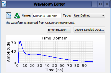
These standards define electronic circuits designed to produce waveforms that mimic real world static discharge events, such as discharges between a human's fingertip and an electronic device (HBM), or between one charged device and another (CDM). Hardware manufacturers are the target audience of these standards, so the excitation circuits are described in detail, but the analytical expressions for ESD waveforms that are needed for software simulation, are not typically provided. Equations must therefore be derived and implemented to generate waveforms that fulfill the requirements defined by each ESD standard ([1]-[8]).
Once the desired ESD waveform is generated, it can be added to the project as a user defined waveform.
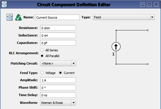
The ESD waveform may then be used to define a current source feed definition. The corresponding circuit component should be placed between the tip of the ESD gun and CAD model geometries.
Circuit Components
It is more common for circuit components to suffer damage from overvoltages and overcurrents during ESD testing than it is for dielectric breakdown to occur, so XF monitors for electronic component failures during ESD testing. Rated voltage and current input parameters, which are obtained from electronic component data sheets, can be added to all circuit component defintion types, such as a passive load. This functionality flags each component that exceeds its rated design parameters and reports to users their susceptibility to permanent damage.
Grid
The primary challenge faced when using FDTD to simulate ESD testing is achieving practical computational requirements. This is because the length of ESD test waveforms is typically long in relation to the FDTD timestep required when resolving the fine detail of many electronic devices. Therefore, the grid definition should be fine enough to resolve important geometric details, but not as fine as is generally required to obtain highly accurate S-parameters and far-zone patterns. For example, it is reasonable for conducting traces to be separated by as little as one or two FDTD cells, and for substrates to be one or two cells thick because ESD simulations are screening for electrostatic potentials between conductors and not high frequency behavior. Users can obtain additional computational savings by reducing the number of free space padding cells and absorbing boundary layers because radiated fields are not of interest.
Sensors
Defining the dielectric strength of a material enables users to monitor FDTD cell edges for potential dielectric breakdown during transient simulations using a dielectric breakdown near-field sensor.
This sensor instructs the calculation engine to monitor cell edges for electric fields that exceed the dielectric strength of their constituent material and record instances at which dielectric breakdown is likely to occur. This sensor requires users to define the free space dielectric strength that will be used for all edges without an assigned material. The default free space dielectric strength value is 3.0 MV/m, which is approximately the dielectric strength of air at sea level. The sensor also allows users to define a bounding box in order to limit the volume that is monitored for dielectric breakdown. Users can therefore obtain computational savings by defining specific areas of interest as opposed to examining the entire computational space. Materials with infinite dielectric strength are ignored by the dielectric breakdown sensor.
Simulation Setup
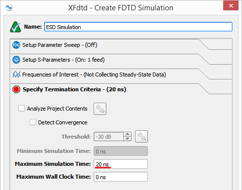
When creating the FDTD simulation, users should disable S-parameter and steady-state data collection because they are not relevant to ESD testing, and the termination criteria must be specified with consideration to the source ESD waveform. For example, when the HBM waveform is a 100 ns pulse, turning off the analyze project contents and detect onvergence features will ensure the simulation does not terminate early. Setting the maximum simulation time to 100 ns will simulate the entirety of the test waveform. However, the majority of dielectric breakdown and circuit component failures occur close to the peak of the ESD pulse. Some computational savings can therefore be obtained by terminating the simulation shortly after the peak amplitude of the pulse, as shown in the image that terminates the simulation at 20 ns rather than 100 ns.
Results
Once the simulation is complete, users can view the locations at risk of experiencing dielectric breakdown during ESD testing.
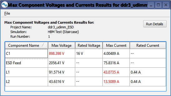
Circuit components that exceeded their rated design parameters during ESD testing, and are therefore susceptible to permanent damage, are also reported. These results predict locations and components at risk of suffering ESD damage, allowing engineers to optimize their designs and formulate ESD mitigation strategies prior to the hardware prototyping stage.
References
- Cerri, G., R. Leo, and V. M. Primiani, "ESD indirect coupling modelling," IEEE Trans. On EMC, 38, pp. 274 - 281, 1996.
- Keenan, R. K., and L. K. A. Rossi, "Some fundamental aspects of ESD testing," Proc. of IEEE Int. Symp. on Electromagnetic Compatibility, pp. 236 - 241, 1991.
- Songlin, S., B. Zengjun, T. Minghong, and L. Shange, "A new analytical expression of current waveform in standard IEC61000-4-2," High Power Laser and Particle Beams, 5, pp. 258 - 271, 2003.
- Yuan, Z., T. Li, J. He, S. Chen, and R. Zeng, "New mathematical descriptions of ESD current waveform based on the polynomial of pulse function," IEEE Trans. on EMC, 48(3), pp. 589 - 591, 2006.
- Wang, K., D. Pommerenke, R. Chundru, T. Van Doren, J. L. Drewniak, and A. Shashindranath, "Numerical modeling of electrostatic discharge generators," IEEE Trans. on EMC, 45(2), pp. 258 - 271, 2003.
- Wang, K., J. Wang, and X. Wang, "Four order electrostatic discharge circuit model and its simulation," TELKOMNIAK, 10(8), pp. 2006 - 2012, 2012.
- Berghe, S. V., and D. Zutter, "Study of ESD signal entry through coaxial cable shields," J. Electrostat., 44, pp. 135 - 148, 1998.
- Lundengard, K., M. Rancic, V. Javor, and S. Silvestrov, "Electrostatic discharge current modelling using multi-peaked analytically extended function," Proc. of 2nd International Multidisciplinary Conference on Computer and Energy Science (SpliTech), pp. 272 - 277, 2017.