Main Website
|
XFdtd
|
WaveFarer
|
Contents
|
Search
|
Log In
Contents
List of webpages in the support site.
Installation
Configure EQI
Configuration and requirements for system administrators.
Demo, Node-Locked, and USB Key Licensing
Setup a license file for XFdtd.
End User Setup for a Compute Cluster
Use external queuing in the XF user interface.
Floating License FAQ
Frequently asked questions about setup and license servers.
Floating License
License multiple machines using a floating license server.
Minidumps
Collect minidumps on Windows.
MPI Cluster Setup
Install XFdtd on an MPI cluster.
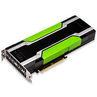
NVIDIA GPU Troubleshooting
Install the newest driver for your graphics card and explore additional options.
rescaleqs.py Documentation
Script configuration for system administrators.
USB Key Drivers
Download and install required drivers.
USB Key FAQ
Frequently asked questions about setup and licensing.
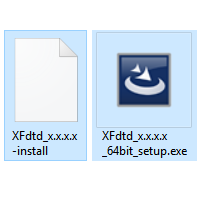
XFdtd Installation
Install the XF application and its supporting files.
Releases
XFdtd Release 7.10.2
Introducing tuning in the schematic editor and more.
XFdtd Release 7.10.1
Introducing frequency bands and more.
XFdtd Release 7.10.0
Introducing the schematic editor and more.
XFdtd Release 7.9.2
Introducing TVS diodes and more.
XFdtd Release 7.9.1
Introducing singularity correction and more.
XFdtd Release 7.9.0
Introducing superposition post-processing and more.
XFdtd Release 7.8.1
Introducing electrostatic discharge analysis and more.
XFdtd Release 7.8.0
Introducing distributed circuit components and more.
XFdtd Release 7.7.1
Introducing updated shortcut capabilities and more.
XFdtd Release 7.7.0
Introducing circuit co-simulation with a netlist component and more.
XFdtd Release 7.6.0
Learn about the wrap sheet feature and more.
XFdtd Release 7.5.1
Learn about Optenni Lab integration and more.
XFdtd Release 7.5.0
Introducing the Circuit Element Optimizer and more.
XFdtd Release 7.4.0
Learn about PrOGrid Project Optimized Gridding™ and more.
Standards
IEC/IEEE 62704-1
Code verification documentation for the IEC/IEEE SAR standard.
IEC/IEEE 63195-2
Code verification documentation for the IEC/IEEE power density standard.
Antenna Design
Analyze Codebook: CDF of EIRP
Bulk-process numerous beam states.
Antenna Group Delay
Compute and plot the single-antenna result.
Antenna Group Delay
Interpret the single-port result.
Antenna Simulation Workflow
Overview of the standard workflow for simulating an antenna.
Antenna Array Use Cases
Analyze beam steering.
CDF of EIRP & Max Hold
Interpret the result.
Near- to Far-Field Transform
Method for computing electric fields in the far-zone.
Optenni Lab Integration
Improve the matching network design process.
Plot Far Zone Statistics
Plot data at multiple frequencies.
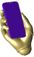
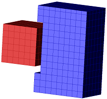
Poseable Hand
Import and reposition CADHuman's Poseable Hand.
Step-By-Step Tutorials
Learn XFdtd with getting-started tutorials.
Getting Started
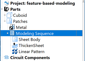
Feature-Based Modeling
Apply modeling operations to geometry.
Flat Parts List
Evaluate and adjust part properties from a single list.
Grid Visualization
Preview the grid's alignment with geometry.
Libraries
Build a collection of reusable objects.
Picker Tools
Select geometry faces, edges, and vertices using tools and hotkeys.
Simulation Workflow
Learn the steps for setting up a simulation.
User-Interface Orientation
Navigate the software and apply commonly used tools and features.
Knowledge Articles
Accurate & Consistent SAR Results
Recommendations for grid alignment.
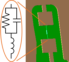
Distributed Circuit Component
Explanation of the component's property.
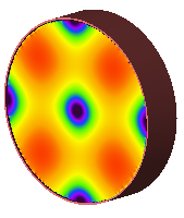
Modal vs. Nodal Waveguide
Comparison of the two waveguide interface excitations.
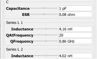
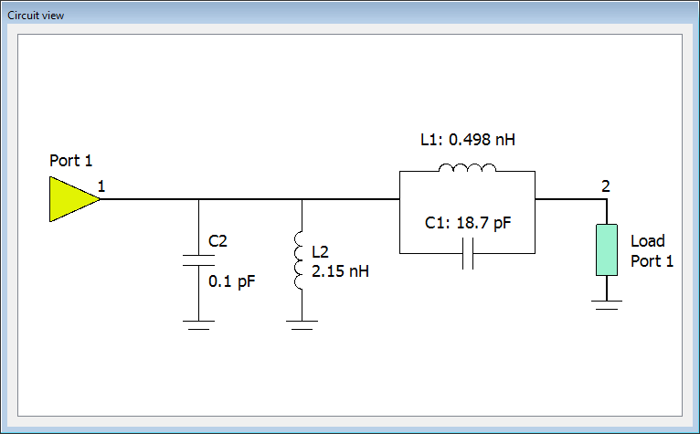
Matching Network Design
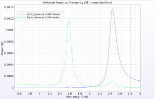
Diplex Matched Antenna
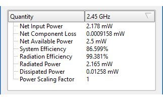
Evaluate delivered power in the GPS and WiFi operating modes.
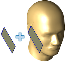
Dynamic Antenna Matching
Proximity sensor-enabled impedance matching of a phone in free space and against a head.
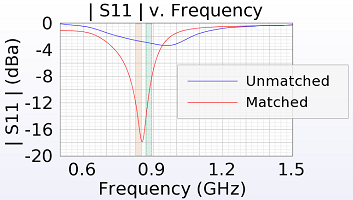
Simple Matching Network
Impedance matching of an L-antenna for LTE Band 5.
Tune a Fixed-Band Match
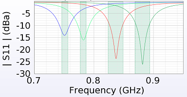
Determine matching network component values for LTE Band 5 using tuning sliders.
Tune a Tunable Match
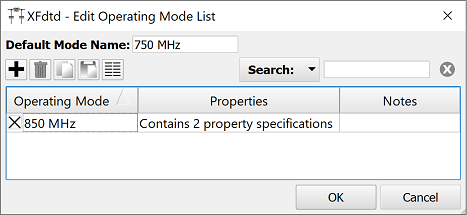
Match component values for multiple operating modes.
Scripts
Compute Average Power Density
Analyze planar sensor results based on IEC/IEEE 63195-2.
Flatten Selected Parts
Remove all features from each part's modeling sequence.
Netlist Library Importer
Import subcircuits as separate netlist component definitions.
Optimization Functions
Optimize parameters using a set of utilities.
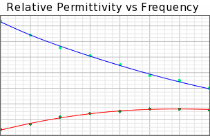
Plot Material Parameters
Generate a graph of a material definition's data sets.
Rename Plots
Recreate the legend without rebuilding the graph.
Workflows
Electrostatic Discharge Analysis
Set up a project for an ESD event.
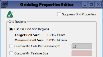
Gridding Workflow
Define XF's grid.
Parameter Sweep Workflow
Perform a parametric analysis.
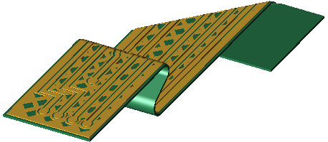
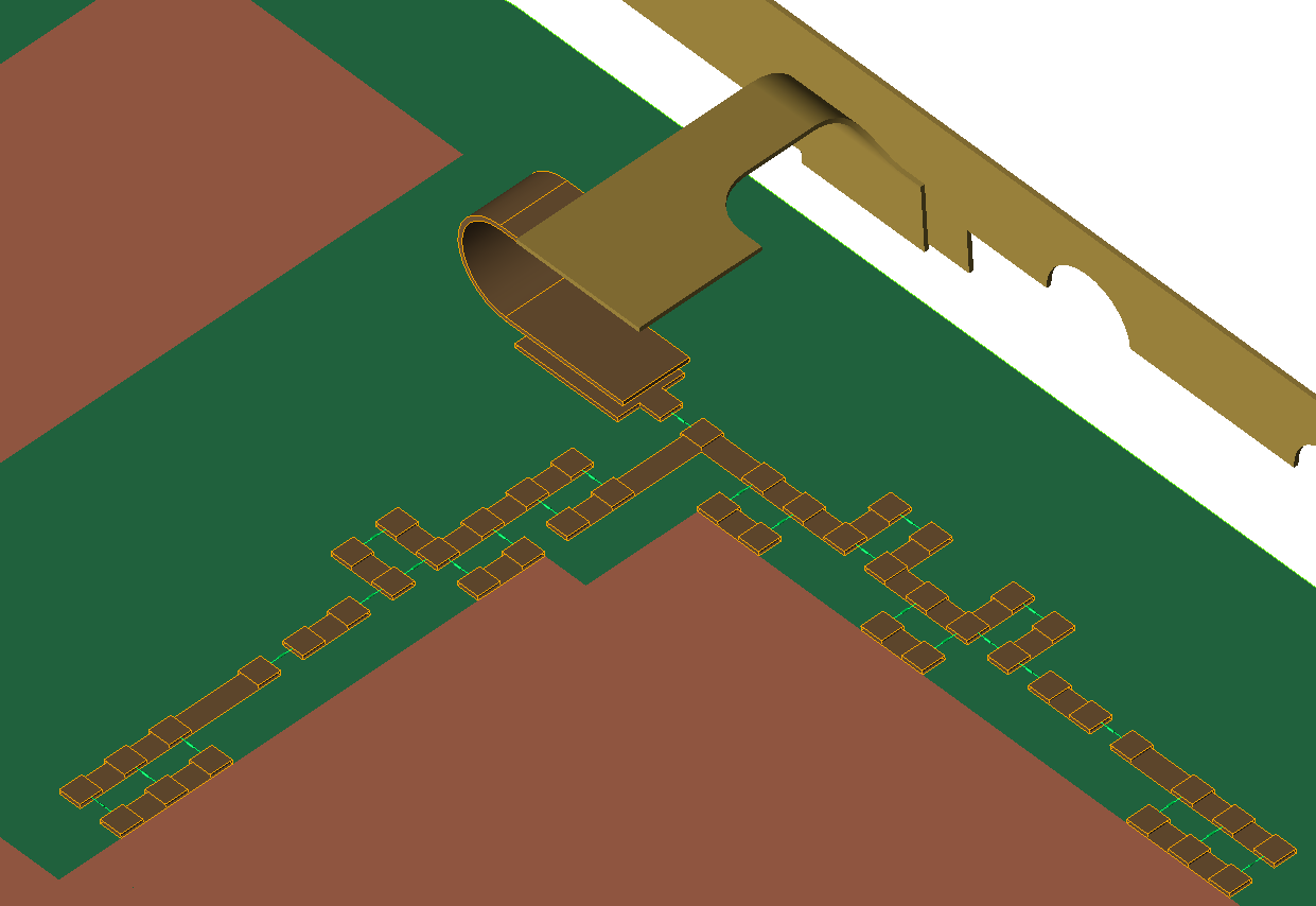
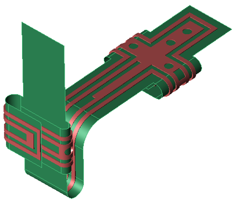
PCB Wrap Workflow
Wrap a multi-layer PCB during import.
SAR Averaging Workflow
Set up a project for averaged SAR analysis.
VOP Compression
Post-process averaged SAR results.
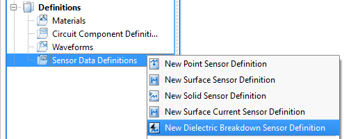
Definitions
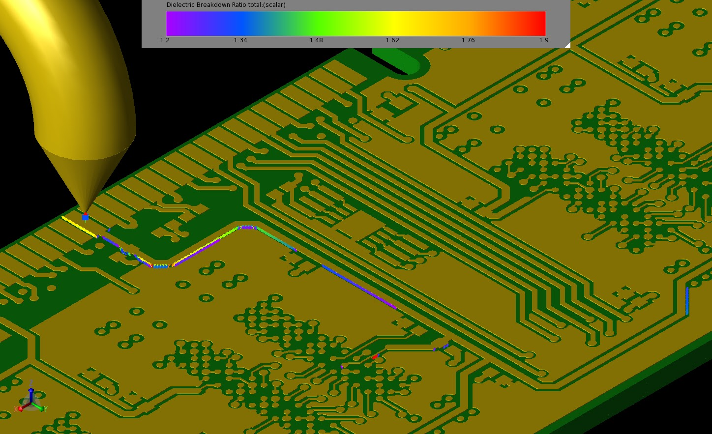
Dielectric Breakdown Sensor Definition
Set the time sampling range to detect breakdown.
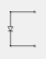
Diode
Model the nonlinear current-voltage curve of a PN junction.
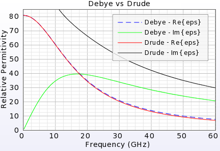
Dispersive Material Calculator
Fit a Debye-Drude material to measured data.
Debye-Drude Material
Electric dispersive material definition.
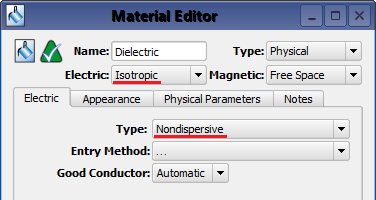
Nondispersive Material
Isotropic material definition with constant properties versus frequency.
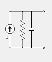
Feed
Define a voltage or current source.
Netlist Component
Define a circuit component as a SPICE model.
Nonlinear Capacitor
Apply nonlinear behavior to a component.
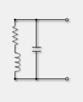
Passive Load
Create an RLC component with no source.
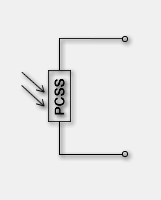
Photoconductive Semiconductor Switch
Define a light-enabled switch.
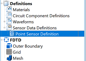
Point Sensor Definition
Set the time-domain data to collect for a point sensor.
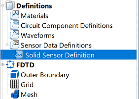
Solid Sensor Definition
Set which data to collect in a 3-D volume.
Surface Conductivity Correction
Maintain the surface impedance for a metal.
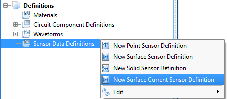
Surface Current Sensor Definition
Request surface current output as a function of time or frequency.
Surface Sensor Definition
Set which data to collect on a 2-D surface.
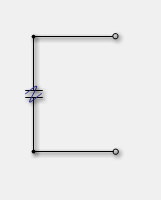
Switch
Add opening and closing switches.
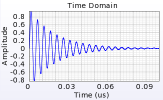
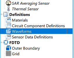
User Defined Waveform
Create a custom waveform definition.
Waveform Editor
Define an excitation's time- and frequency-domain content.
Excitations
Circuit Components
Specify the location of a lumped component.
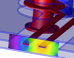
Modal Waveguide Excitation
Excite a waveguide structure with TEM, quasi-TEM, TE, or TM modes.
Nodal Waveguide Excitation
Specify pins for exciting a transmission line.
Plane Wave Excitation
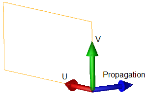
Define the incident direction and polarization.
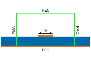
Waveguide Boundaries
Set the outer edges of a waveguide interface.
Waveguide Geometry
Position and size a waveguide interface within the problem space.
General
Coordinate Systems
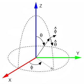
Angle and vector component definitions.
Graphs
View and manipulate 2-D plotted results.
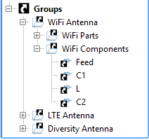
Groups
Create and edit shortcut groups in the project tree.
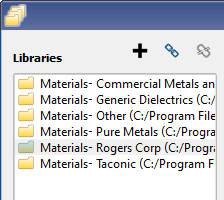
Libraries
Create reusable collections of objects and definitions.
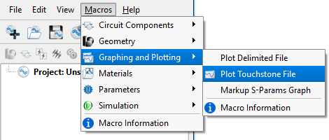
Macros Menu
Register macros with XF for use in all projects.
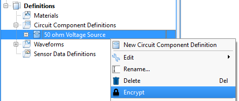
Object Encryption
Password-protect geometry, material, and circuit component parameters.
Outer Boundary
Apply conditions at the edges of the simulation space.
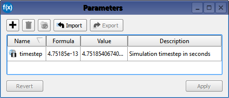
Parameters Window
Define universal parameters.
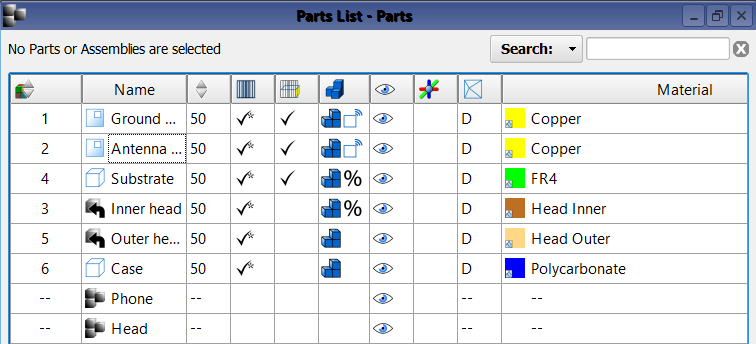
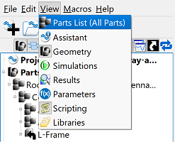
Parts List
View and modify geometric parts' properties through a flat list.
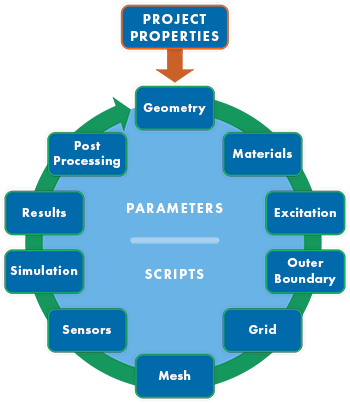
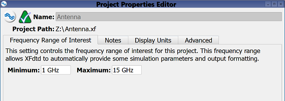
Project Properties
Specify settings used throughout a project.
Geometry
Check Model
Identify issues with a 3-D CAD model.
Detach Modeling Option
Control one part's dependence on another.
Faceting Properties
Control faceting options for parts.
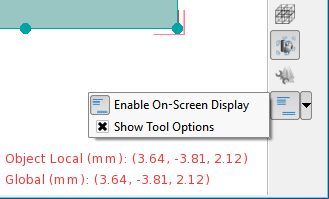
On-Screen Display
View tool-specific information in the geometry window.
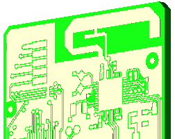
PCB Import
Import ODB++ and Allegro .brd files.
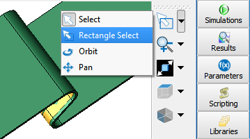
Rectangle Select Tool
Select multiple parts at once.
Remove Holes
Close gaps in a part.
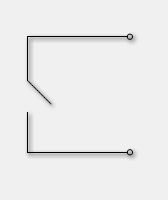
Sheet Body from Edges
Create a sheet body from a closed circuit of edges.
Slice
Cut a part in two.
Thicken Sheet
Turn a sheet into a solid by adding thickness.
Wrap Sheet
Wrap a part onto another.
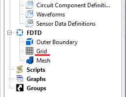
Grid
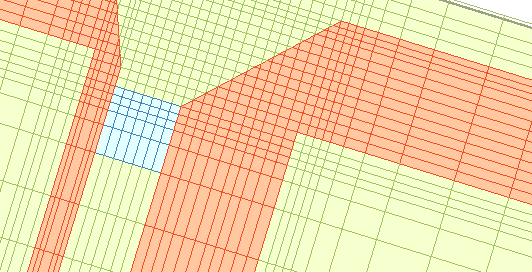
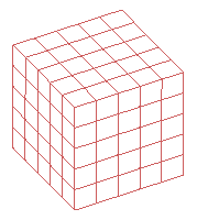
Gridding Algorithm
Discretize the 3-D simulation space and CAD geometry.
Main Grid Editor
Discretize the simulation space.
Part Gridding Properties
Define the grid settings for an individual part.
Mesh
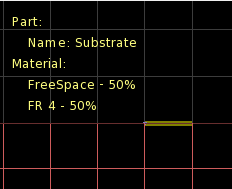
Dielectric Volume Averaging
Enable meshing for dielectric parts.
Mesh View Controls
Render 2-D mesh cutplanes or the entire 3-D mesh.
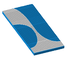
Meshing Order
Prioritize meshing of co-incident, overlapping, and intersecting parts.
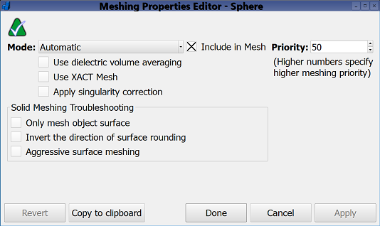
Part Meshing Properties
Adjust the mesh settings for an individual part.
Singularity Correction
Resolve the highly varying fields near metallic edges.
Touching Objects
Identify and separate intersecting objects in the mesh.
Results
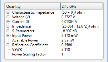
Circuit Component Results
Discrete frequency results for active and passive circuit components.
SAR Combination
Combine SAR results to find a maximum SAR value.
Sequence Tab
View animated results.
System Sensor
Discrete frequency results for the system sensor.
UAN File Format
Learn about a 3-D far zone radiation pattern text file.
Volumetric SAR File Format
Learn about binary file format.
Schematics
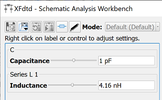
Analysis Workbench
Tune component values and view the updated results.
Basic Components
Set the properties of schematic elements, such as source, RLC, and FDTD blocks.
Hotkeys
Shortcuts in the schematic editor.
Operating Modes
Define various states of a schematic.
Schematic Editor
Define schematics and run a frequency-domain circuit solver.
Schematic Results
Frequency-domain circuit solver's AC and S-parameter results.
Transmission Line Components
Set the properties of schematic elements.
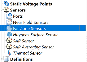
Sensors
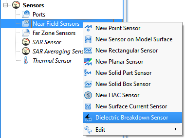
Dielectric Breakdown Sensor
Request results for electrostatic discharge.
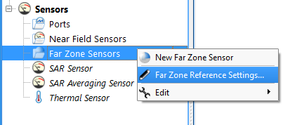
Far Zone Reference Settings
Set the phase reference point for far zone sensors.
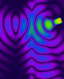
Far Zone Sensor
Request data outside the simulation space.
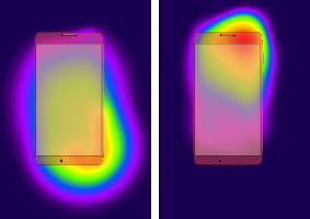
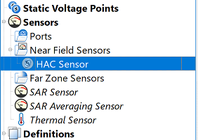
HAC Sensor
Collect data for analyzing hearing aid compatibility.
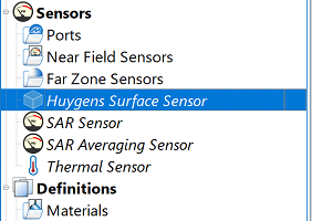
Huygens Surface Sensor
Record data for use in Wireless InSite.
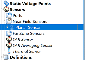
Planar Sensor
Record data on a plane through the space.
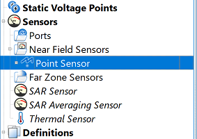
Point Sensor
Record data at a specific point in space.
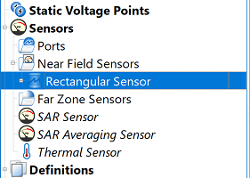
Rectangular Sensor
Record data on a rectanglar surface in space.
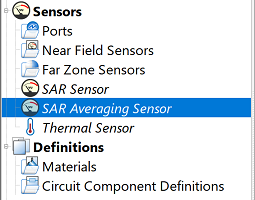
SAR Averaging Sensor
Compute 1-gram and 10-gram averaged SAR.
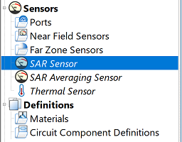
SAR Sensor
Measure the unaveraged SAR in dielectric materials.
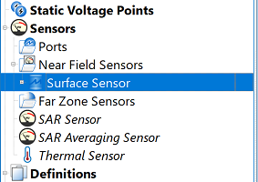
Sensor on Model Surface
Collect data on one or more faces of a part.
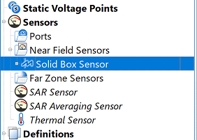
Solid Box Sensor
Record data throughout a 3-D box.
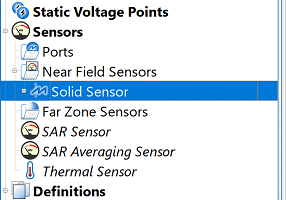
Solid Part Sensor
Record data throughout a part's volume.
Surface Current Sensor
View the electrical current on a metal surface.
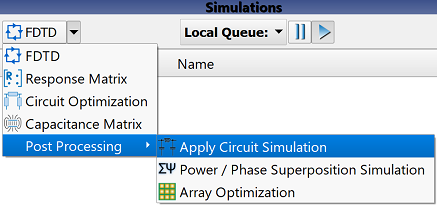
Simulations
Apply Circuit Simulation
Combine a circuit schematic with FDTD results.
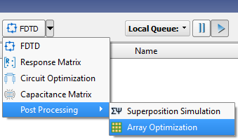
Create Array Optimization
Determine optimal port phases for an array.
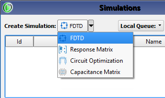
Create FDTD Simulation
Set up and run a calculation.
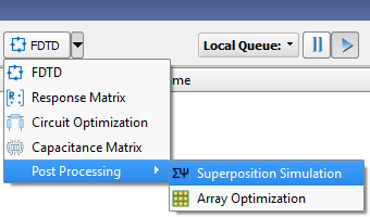
Create Superposition Simulation
Combine steady-state results.
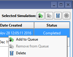
Manage Simulations
Options for queuing, deleting, and editing existing simulations.
Installation
Demo, Node-Locked, and USB Key Licensing
Setup a license file for WaveFarer.
Floating License FAQ
Frequently asked questions about setup and license servers.
Floating License
License multiple machines using a floating license server.
USB Key Drivers
Download and install required drivers.
USB Key FAQ
Frequently asked questions about setup and licensing.
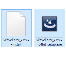
WaveFarer Installation
Install the WaveFarer application and its supporting files.
Releases
WaveFarer Release 2.1.0
Introducing diffuse scattering and more.
WaveFarer Release 2.0.0
Introducing automotive radar simulation.
Knowledge Articles
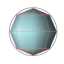
Corner Reflector Equations
Geometric relationship to a pyramid defined.
Well-Constructed Target Models
Guidelines for generating precise CAD geometry.
Scripts
Create Linear Chirp Simulation
Create a simulation that analyzes multiple chirps per frame.
Export Complex Impulse Response
Export data from a simulation to MATLAB.
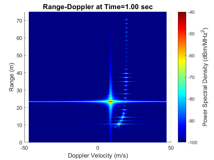
Generate Range-Doppler
Post-process a linear chirp simulation.
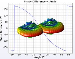
Plot Phase Difference
Compute the phase difference between two plots.
Plot Received Power Versus Parameter
Compare received power versus either distance or angle in a graph.
Getting Started
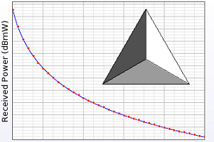
Corner Reflector
Compare the received power versus distance to the radar range equation.
Euro NCAP Vehicle Target
Simulate a linear chirp and export results for post-processing.
User-Defined Antennas
Import custom radiation patterns and verify their placement.